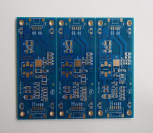
Today I'd like to delve a bit into China PCB manufacturer -JLCPCB’s PCB pricing,quality, features, delivery. As we all known, PCB price of JlCPCB is the cheapest among China PCB Manufacturers. I think we get PCB easier and spend less than the past. Lots of manufacturers are gradually adopting the so called Perfect Test system to achieve a top precision layer alignment. According to test a certain number of prototype printed circuit boards, the test system determines the average design clearance between the pattern and holes that connect the sheets. The results are
processed and then when you start the actual production process, the system will have calculated the best alignment and give you high precision multilayer PCB products that you will be proud of. Such as ordering on JLCPCB is very easy, just uploading your gerber files.
processed and then when you start the actual production process, the system will have calculated the best alignment and give you high precision multilayer PCB products that you will be proud of. Such as ordering on JLCPCB is very easy, just uploading your gerber files.
JLPCB Price
In generally, China PCB manufacturers are cheaper than European PCB manufacturers. However the price is amazing in JLCPCB.
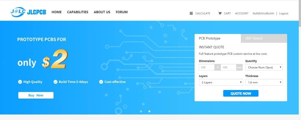
$2 for 10 pcs of customized pcb? That’s a amazing deal! It’s really in JLCPCB.
In short, a lot: $2 for 10 copies, 2 layers, max 100 x 100mm pcb size, a choice of six colors (green, red, yellow, blue, white and black),FR4-Standard Tg 140C,double-sided or single or no silkscreening, HASL(with lead), finish. I’d say that’s enough to tempt even the most ardent home etcher….
JLCPCB Quality
Vias
|
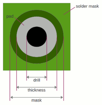
Via - a hole in a board used to pass a signal from one layer to another. Tented vias are covered by soldermask to protect them from being soldered to. Vias where connectors and components are to be attached are often untented (uncovered) so that they can be easily soldered.
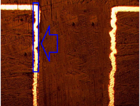
For backplane designs, the most common form of vias use plated through hole (PTH) technology. They connect the pins of connectors to inner signal layers. JLCPCB now only make Plating Through Hole(PTH). Finished copper thickness on the printed circuit board is an important index of via .According to standard hole copper thickness can't be lower than 18um .TheJlcocb average copper thickness is 20um higher than the national standard. The too thin hole copper thickness will affect operating current size. On the boards from JLCPCB I couldn’t see any obvious imperfections or find any shorts. Traces are crisp and as far as I can tell all vias were well plated. |
Pads
|
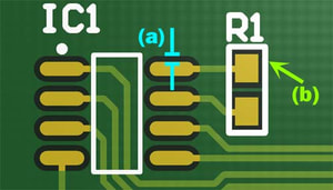
Pad - a portion of exposed metal on the surface of a board to which a component is soldered.
A pad is a small surface of copper in a printed circuit board that allows soldering the component to the board. You can think of a pad as a piece of copper where the pins of the component are mechanically supported and soldered. JLCPCB applies Copper Hatching if your PCBs designed with Pads. Pad etching looks good. A HASL (hot air solder leveling) finish solders fine. |
Silkscreen or Overlay
|
Silk-screening is the process where the manufacturer prints information on the soldermask conducive to facilitate the processes of assembly, verification and repair. Generally the silkscreen is printed for indicating test points as well the position, orientation and reference of the electronic components that are part of the circuit. Also it can be used for any purpose that the designer may require, for example, the company name, configuration instructions (this was commonly used in old PC motherboards), etc. The silkscreen can be printed on both surfaces of the board. Also the term silkscreen is known as overlay. Figure 2 shows a region of a circuit, all the printings made in white correspond to the silkscreen.
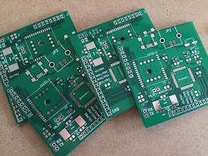
JLCPCB board silkscreen is put on both sides, resolution is good and easily readable. |
Soldermask(PCB color)
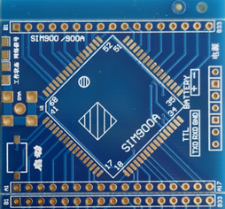
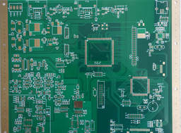
Soldermask - a layer of protective material laid over the metal to prevent short circuits, corrosion, and other problems. All I can tell you is that JLCPCB boards soldermasks are nicely applied and they have six colors.The color is crisp but will still allow you to follow underlying copper tracks, well.
JLCPCB Production and Shipping
JLCPCB does well in keeping you informed of production updates: I placed my order on 12th Sep. and received production updates on the 13th,Sep. and the 15th Sep. (order shipped). Thumbs up for staying within the suggested production time of 4 working days!
Onto shipping: I usually go for DHL because of it’s acceptable price and very fast delivery time, only paid about $23 for 4-6 working day shipping to the Netherlands. DHL picked up the pcb’s in Shenzen on 15th Sep. and I received the package on the 20th Sep..
Overall, JLCPCB is one of best China PCB manufacturers. The PCB from JLCPCB is much pretty perfect .The ordering process are so good that I didn't even mention it. I just hope that its price still give me a surprise.


